
Контрактное производство электроники под ключ в Китае
Шэньчжэнь, район Баоань, улица Фуюн, улица Фуцяо, район 3, промышленный парк Лонгхуй 6


SMT basic process elements: solder paste printing -> Parts mounting --> Reflow welding --> AOI Optical Detection --> Maintenance --> The board is divided.
Some people may ask why it is so complicated to connect an electronic component. In fact, this is closely related to the development of our electronic industry. Nowadays, electronic products pursue miniaturization, and the previously used punch plug-in components can not be reduced. The function of electronic products is complete, the integrated circuit(IC) used has no perforated components, especially large scale, high integration IC, have to use surface patch components.
Product mass, production automation, the factory to low cost and high output, produce products to meet customer needs and strengthen the market competitiveness of the development of electronic components, integrated circuit (IC) development, semiconductor materials of multiple applications. Electronic science and technology revolution is imperative, the pursuit of the trend. It can be imagined that the development of smt surface assembly technology and technology is inevitable in the case that intel,amd and other manufacturers of cpu and image processing devices have improved their production process to more than 20 nanometers.

SMT patch processing advantages: high assembly density, small size of electronic products, light weight, the size and weight of the patch components is only about 1/10 of the traditional plug-in components, generally after the adoption of SMT, the size of electronic products reduced by 40%~60%, 60%~80% weight reduction. High ** ** ability, strong vibration resistance. Low defect rate of solder joint. Good high frequency characteristics. Electromagnetic and radio frequency interference is reduced. Easy to realize automation, improve production efficiency. Reduce the cost by 30%~50%. Save materials, energy, equipment, manpower, time, etc.
It is precisely because of the complex technological process of smt patch processing that there are many smt patch processing factories. In Shenzhen, thanks to the booming development of the electronic industry,smt patch processing has achieved a prosperity of the industry.
(1) Visual inspection Visual inspection is the use of human eyes to carry out some simple inspection, such as surface dents, pits, scratches, etc. * It is important to check whether the weld hole is in the center of the pad and the integrity of the wire pattern.
(2) Connectivity through holes For multi-layer circuit boards to conduct connectivity tests, the purpose is to find out whether the PCB graphics have connectivity.
(3) Insulation resistance of the circuit board Insulation resistance is a resistance of the printed circuit board insulation components to the external DC voltage. Choose two or more wires with close spacing and insulation, first measure the insulation resistance between them, after humidifying and heating for a period (the relative humidity in the box is about 45 degrees Celsius, 10 hours to two days), put them in the room for one hour, and then measure the insulation resistance between them.
(4) Weldability of welding pad Weldability is used to measure the wetting ability of solder on printed graphics when components are welded to the printed circuit board, which is generally expressed by wetting, semi-wetting and non-wetting. When wet, the solder can flow and expand freely on the wire and pad to form adhesive connection. Semi-wetting, the solder first wets the surface of the pad, and then forms the solder ball in some irregular places of the pad because of improper wetting. Without wetting, the solder accumulates on the surface, but does not form an adhesive connection to the pad surface.
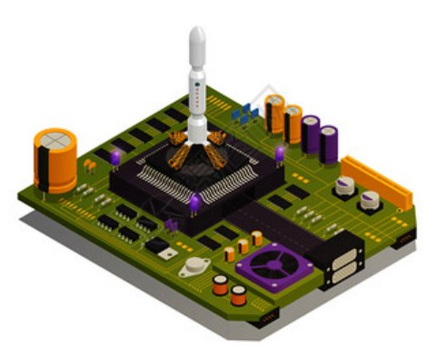
Surfacemount technology (SMT) is a new generation of electronic assembly technology developed from hybrid integrated circuit technology. It is characterized by surface mounting of components and reflow welding technology. It has become a new generation of assembly technology for electronic products manufacturing.
The wide application of SMT promotes the miniaturization and multi-function of electronic products, and provides conditions for mass production and low defect rate production. SMT is surface assembly technology, which is a new generation of electronic assembly technology developed from hybrid integrated circuit technology.
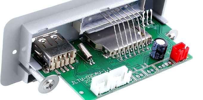
The main components of the SMT production line are: surface assembly components, electric subgrade board, assembly design, assembly process;
The main production equipment includes printing machine, dispensing machine, paste machine, reflow welding furnace and wave welding machine. The equipment includes testing equipment, repair equipment, cleaning equipment, drying equipment and material storage equipment.


Достаточно загрузить файлы Gerber, BOM и проектные документы, и команда KINGFORD предоставит полное предложение в течение 24 часов.