
Контрактное производство электроники под ключ в Китае
Шэньчжэнь, район Баоань, улица Фуюн, улица Фуцяо, район 3, промышленный парк Лонгхуй 6

In the printed circuit board, copper is used to interconnect components on the substrate. Although it is a good conductor material to form the pattern of the conductive path of the printed circuit board, if it is exposed to air for a long time, it is also easy to lose luster due to oxidation and lose weldability due to corrosion. Therefore, a variety of techniques must be used to protect copper printed wire, through hole and plated through hole, including organic coating, oxide film and electroplating techniques.
Organic lacquers are very simple to apply, but are not suitable for long-term use due to changes in concentration, composition and curing period, and can even lead to unpredictable deviations in weldability. The oxide film protects the circuit from erosion, but it does not maintain weldability. Electroplating or metal coating processes are standard operations to ensure weldability and protect circuits from erosion, and play an important role in the manufacture of single sided, double sided and multilayer printed circuit boards. In particular, it has become a standard operation to provide welding protection for copper printed wire by plating a layer of welding metal. Keyou specialized in the production of PCB circuit board, LED aluminum substrate, copper substrate, carbon fiber board, etc.

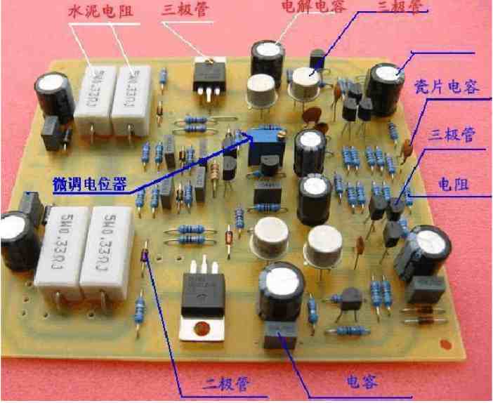
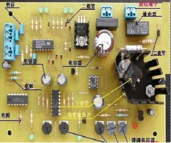
Printed circuit board
The interconnection of various modules in electronic equipment often requires the use of printed circuit board plug sockets with spring contacts and matching designs of printed circuit boards with connected contacts. These contacts should have high wear resistance and very low contact resistance, which requires a coating of rare metals, of which gold is the most commonly used metal. In addition, other coated metals can be used on the printed line, such as tin plating, plating, and sometimes copper plating in some areas of the printed line.
The other coating on copper printing wire is organic material, usually a solderproof film, which is screened over an epoxy resin film where no welding is required. The process, which is coated with an organic flux protector, does not require electron exchange. When the circuit board is immersed in a chemical bath, a nitrogen-tolerant compound can attach to the exposed metal surface without being absorbed by the substrate.
The precision technology required by electronic products and the strict requirements of environmental and safety adaptability have prompted the practice of electroplating to make great progress, which is obviously reflected in the manufacture of high complexity and high resolution multi-substrate technology. In electroplating, electroplating technology has reached a very high level through the development of automated, computer-controlled electroplating equipment, the development of highly sophisticated instrumentation for chemical analysis of organics and metal additives, and the emergence of technologies for precise control of chemical reaction processes.
There are two standard ways to make the metal layer grow in the circuit board wires and through holes as follows:
1. Line plating
The process accepts the formation of copper layers and etching resistance metal plating only where circuit patterns and through-holes are designed. During line plating, the width of each side of the line and pad increases roughly as much as the thickness of the plating surface, so there is a need to leave a margin on the original negative.
In line plating basically most of the copper surface to be blocked, only in the line and welding pad circuit graphics where electroplating. The required capacity of the power supply current is usually greatly reduced because the surface area to be plated is reduced, and when using a contrast reversal photosensitive polymer dry film plating inhibitor (one of the most commonly used types), the negative negative can be made with a relatively inexpensive laser printer or drawing pen. The anode consumes less copper in line plating, and less copper needs to be removed in the etching process, thus reducing the analysis and maintenance costs of the electrolytic cell. The disadvantage of this technique is that the circuit pattern needs to be coated with tin/lead or an electrophoretic resistance material before etching and removed before soldering resistance is applied. This adds complexity and an additional set of wet chemical solutions.
2. All plates are plated with copper
In this process, all surface areas and boreholes are plated with copper, some resistance is poured on the surface of the unwanted copper, and then etching resistance metal is plated. Even for a medium-sized printed circuit board, this requires a considerable amount of current to be mined to produce a smooth, bright copper surface that is easy to clean and can be used in subsequent processes. If a photoplotter is not available, negative negatives need to be used to expose circuit graphics, making it a more common contrast reversal dry film photoresist.


Достаточно загрузить файлы Gerber, BOM и проектные документы, и команда KINGFORD предоставит полное предложение в течение 24 часов.