
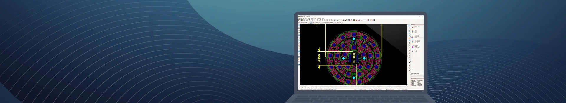
- Возможности проектирования печатных плат
Возможности проектирования & компоновки печатных плат | ||||
Минимальная ширина трассы: | 2.5mil | Минимальное расстояние между следами | 2.5mil | |
Мин.переход: | 6mil(лазерное сверление 4mil ) | Макс. слой | 48 слоев | |
Минимальное расстояние между BGA | 0.35mm | Макс. Контакт BGA | 3600pin | |
Макс.высокоскоростной сигнал | 40 GBPS | Самое быстрое время доставки | 6 часов/ Item | |
HDI Самый высокий слой | 22 слоя | HDI Верхний слой | 14 слоев любой слой HDI | |
Время выполнения дизайна & макета печатной платы | ||||
Количество контактов на плате | 0-1000 | Срок выполнения проекта (рабочие дни) | 3-5 дней | |
2000-3000 | 5-8 дней | |||
4000-5000 | 8-12 дней | |||
6000-7000 | 12-15 дней | |||
8000-9000 | 15-18 дней | |||
10000-12000 | 18-20 дней | |||
13000-15000 | 20-22 дня | |||
16000-18000 | 22-25 дней | |||
18000-20000 | 25-30 дней | |||
Максимальная пропускная способность | 10000Pin/7 дней | |||
PS:Вышеуказанная дата доставки является обычной датой доставки, и точная дата доставки проекта должна быть всесторонне оценена в соответствии с количеством компонентов, сложностью, слоями и другими факторами печатной платы! | ||||

System advanced training, from beginners to experts, there are various technical special trainings every week

High-standard confidentiality measures, signing confidentiality agreements, and all documents exporting must be approved to ensure that 100% of documents are not leaked.

With a strict quality system process and a strict review system, we have zero error rate quality requirements for PCB design.

PCB design team with an average of more than 12 years of work experience, with complete design software, such as Cadence Allegro\ORCAD, Mentor WG\PADS, etc.

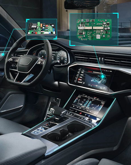


Consumer Lighting, Consumer Electronics, Telecommunications, Transportation, Medical.